Purpose
The RT6200 is a high voltage Buck converter that can deliver up to 0.6A output current from a wide input voltage range of 4.5V to 36V. This document explains the function and use of the RT6200 evaluation board (EVB) and provides information to enable operation and modification of the evaluation board and circuit to suit individual requirements.
Introduction
General Product Information
The RT6200 is a high voltage Buck converter that can support the input voltage range from 4.5V to 36V and the output current can be up to 0.6A. Current mode operation provides fast transient response and eases loop stabilization. The chip also provides protection functions such as cycle-by-cycle current limit and thermal shutdown protection. The RT6200 is available in the SOT-23-6 package.
Product Feature
- Wide Operating Input Voltage Range : 4.5V to 36V
- Adjustable Output Voltage Range : 0.8V to 15V
- 0.6A Output Current
- 0.35Ω Internal Power MOSFET Switch
- High Efficiency up to 95%
- 1.2MHz Fixed Switching Frequency (Duty <90%)
- Support duty up to 95%
- Stable with Low ESR Output Ceramic Capacitors
- Thermal Shutdown
- Cycle-By-Cycle Over-Current Protection
Key Performance Summary Table
|
Key Features
|
Evaluation Board Number: PCB008_V1
|
|
Default Input Voltage
|
12V
|
|
Max Output Current
|
0.6A
|
|
Default Output Voltage
|
5V
|
|
Default Marking & Package Type
|
RT6200GE
|
|
Operation Frequency
|
Steady 1.2MHz at all loads
|
|
Other Key Features
|
4.5V to 36V Input Voltage Range
Support duty up to 95%
|
|
Protection
|
Cycle-By-Cycle Over Current Protection
Thermal Shutdown
|
Bench Test Setup Conditions
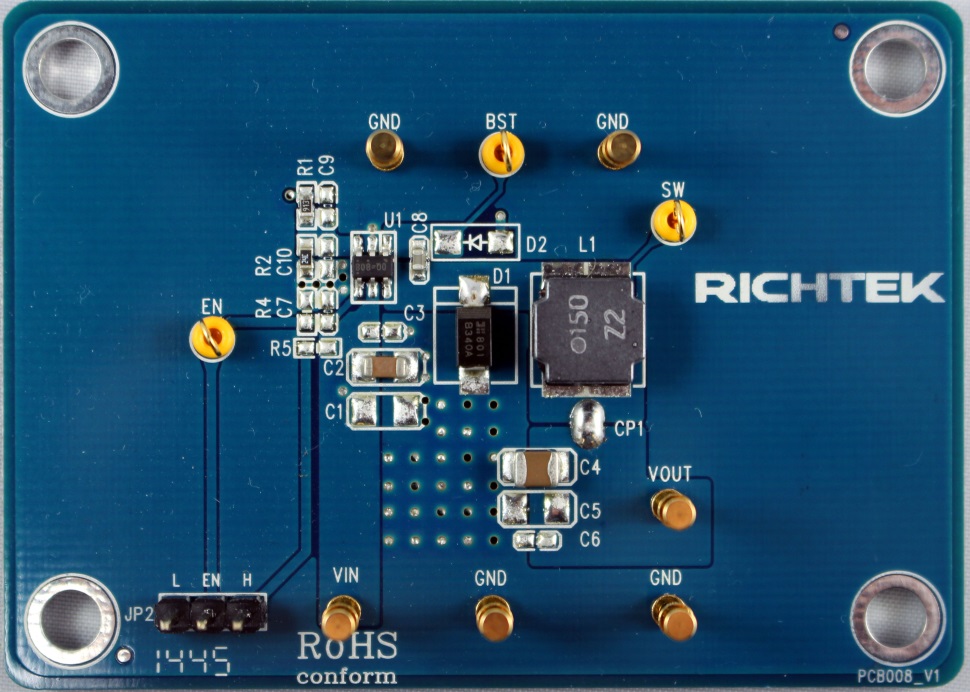
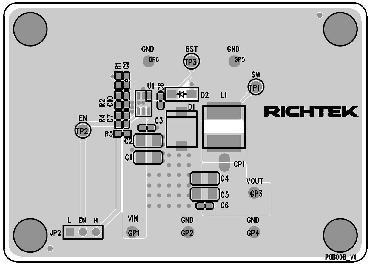
Headers Description and Placement
Please carefully inspect the EVB IC and external components, comparing them to the following Bill of Materials, to ensure that all components are installed and undamaged. If any components are missing or damaged during transportation, please contact the distributor or send e-mail to evb_service@richtek.com
Test Points
The EVB is provided with the test points and pin names listed in the table below.
|
Test point/
Pin name
|
Signal
|
Comment (expected waveforms or voltage levels on test points)
|
|
VIN
|
Input voltage
|
Input voltage range= 4.5V to 36V
|
|
VOUT
|
Output voltage
|
Default output voltage = 5.0V
Output voltage range= 0.8V to 15V
(see ‘’Output Voltage Setting’’ section for changing output voltage level)
|
|
SW
|
Switching node test point
|
SW waveform
|
|
EN
|
Enable test point
|
Enable signal. EN is automatically pulled high by internal circuit to enable operation. Connect EN low (or by R4 pull low resistor) to disable operation.
|
|
BST
|
Boot strap supply test point
|
Floating supply voltage for the high-side N-MOSFET switch
|
|
GND
|
Ground
|
Ground
|
Power-up & Measurement Procedure
1.Apply a 12V nominal input power supply (4.5V < VIN < 36V) to the VIN and GND terminals.
2.The EN voltage is pulled to logic high by internal circuit to enable operation. Drive EN high (>2.5V) to enable operation or low (<0.4V) to disable operation.
3.There is a 3-pin header JP2 “EN” for enable control. To use a jumper at “H” option to tie EN test pin to input power VIN for enabling the device. Inversely, to use a jumper at “L” option to tie EN test pin and ground GND for disabling the device.
4.Verify the output voltage (approximately 5.0V) between VOUT and GND.
5.Connect an external load up to 0.6A to the VOUT and GND terminals and verify the output voltage and current.
Output Voltage Setting
Set the output voltage with the resistive divider (R1, R2) between VOUT and GND with the midpoint connected to FB. The output is set by the following formula:
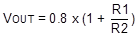
The installed VOUT capacitor (C4) is 22μF, 16V X5R ceramic types. Do not exceed their operating voltage range and consider their voltage coefficient (capacitance vs. bias voltage) and ensure that the capacitance is sufficient to maintain stability and provide sufficient transient response for your application. This can be verified by checking the output transient response as described in the RT6200 IC datasheet.
Schematic, Bill of Materials & Board Layout
EVB Schematic Diagram
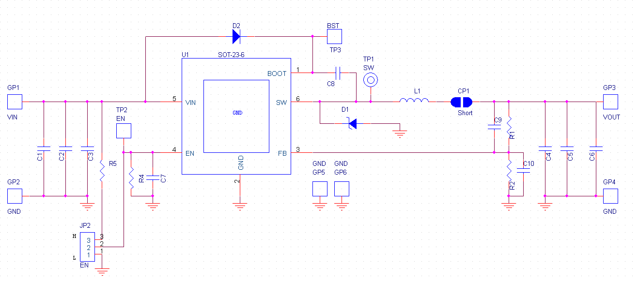
C2: 10μF/50V/X5R, 1206, TDK C3216X5R1H106K
C4: 22μF/16V/X5R, 1210, Murata GRM32ER61C226K
L1: 15μH TAIYO YUDEN NR8040T150M, DCR=50mΩ
Bill of Materials
|
Reference
|
Qty
|
Part number
|
Description
|
Package
|
Manufacture
|
|
U1
|
1
|
RT6200GE
|
DC-DC Converter
|
SOT-23-6
|
RICHTEK
|
|
C2
|
1
|
C3216X5R1H106K160AB
|
10μF/±10%/50V/X5R
Ceramic Capacitor
|
1206
|
TDK
|
|
C4
|
1
|
GRM32ER61C226KE20#
|
22μF/±10%/16V/X5R
Ceramic Capacitor
|
1210
|
Murata
|
|
C8
|
1
|
GRM32MR71H103KA01#
|
10nF/±10%/50V/X7R
Ceramic Capacitor
|
0603
|
Murata
|
|
L1
|
1
|
NR8040T150M
|
15μH/2.7A/±20%, DCR=50mΩ, Inductor
|
8mmx8mmx4mm
|
TAIYO YUDEN
|
|
R1
|
1
|
|
91kΩ/±1%, Resistor
|
0603
|
|
|
R2
|
1
|
|
17.4kΩ/±1%, Resistor
|
0603
|
|
|
CP1
|
1
|
|
Short
|
|
|
|
D1
|
1
|
B340A
|
40V/3A Schottky Diode
|
|
Diodes
|
|
JP2
|
1
|
|
3-Pin Header
|
|
|
|
C1, C3, C5, C6, C7, C9, C10, R4, R5, D2
|
0
|
|
Not Installed
|
0603
|
|
|
TP
|
3
|
BST, SW, EN
|
Test Pin
|
|
|
|
GP
|
6
|
VIN, GND, VOUT, GND, GND, GND
|
Golden Pin
|
|
|
EVB Layout
Top View (1stlayer)
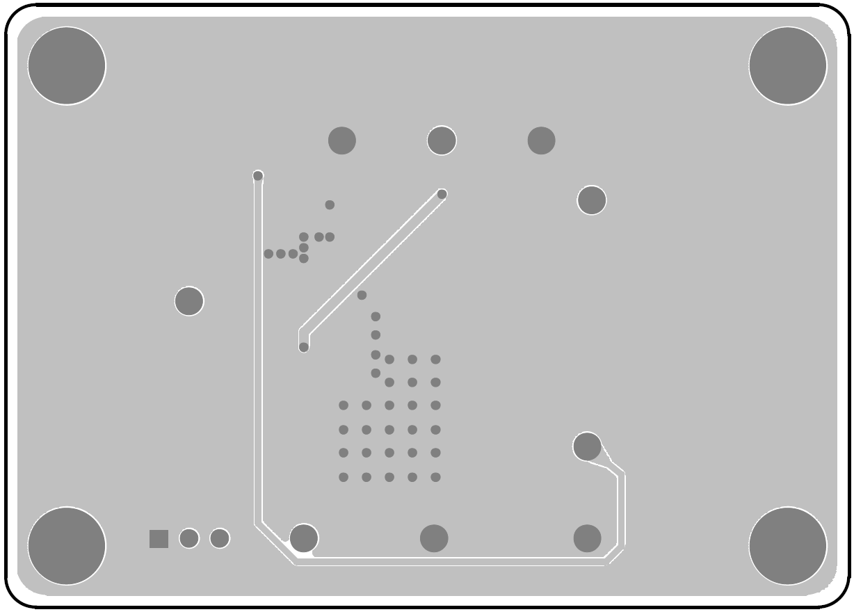
Bottom View (4th Layer)
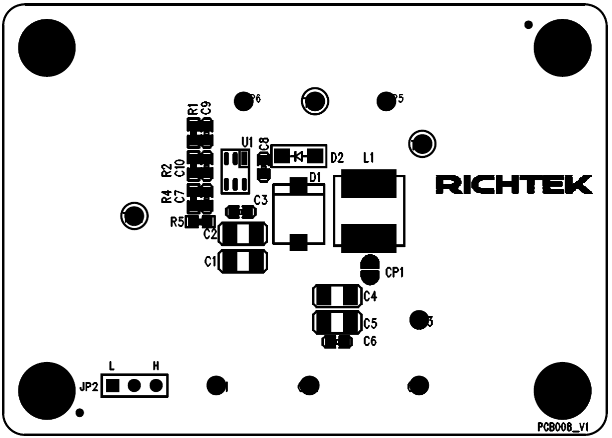
Component Placement Guide—Component Side (1stlayer)
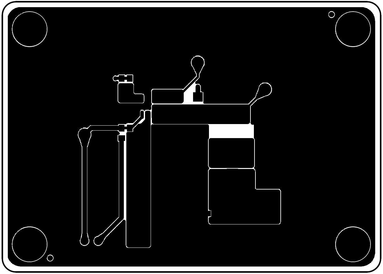
PCB Layout—Component Side (1stLayer)
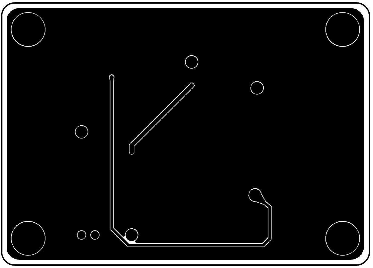
PCB Layout—Bottom Side (4th layer)